Laser-Connect:
Ultrafast laser processing of thin film interconnections in microelectronic, display, and photovoltaic applications

Laser-Connect is an Industry-Academia Partnership and Pathways (IAPP) project funded under the Marie Curie Actions programme in EU FP7.
Project Timeframe: June 2010 - May 2014
Project Timeframe: June 2010 - May 2014
Project Aims
Laser-Connect addresses the generation and exchange of knowledge at the interface of thin film electronic manufacturing and short pulse laser material interactions. The project is highly relevant to the development of new intelligent manufacturing processes in Europe; the technology targets the efficient production of consumer products based on touch panel screens, high density circuit boards, and photovoltaics.
Microelectronics

Implement new high repetition rate short pulse laser processes for structuring high density circuit boards in industry:
- To demonstrate the fabrication of more precise embedded conducting tracks, on the order of microns, with a single step ultrafast laser process.
- To investigate the application of tailored ps and fs pulse trains to optimise the formation of via holes and in reducing the damage to the stopping layers formed by buried metal contacts or landing sites.
Photovoltaics
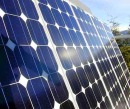
Investigate the application of ps and fs sources in the fabrication of photovoltaics:
- To reduce the heat affected zone associated with nanosecond laser processing of metal and semiconductor alloys by applying new short pulse laser processes with optimised beam delivery.
- To minimise the damage caused during laser ablation to the underlying flexible organic layers by employing ultrafast technologies and on-line diagnostics.
Display

Develop new industrial laser processes for improved manufacture of next generation displays and touch panels:
- To investigate laser ablative thin film removal on glass and polymer surfaces
- To demonstrate improved depth control of laser ablative processes using fs and ps laser pulses.
- To investigate laser ablative thin film removal on glass and polymer surfaces
- To demonstrate improved depth control of laser ablative processes using fs and ps laser pulses.
|

|